Israel's Tower Semiconductor Bets Over 600 Billion Yen on Japan Silicon Photonics Push in Toyama and NiigataA · FULL TRANSLATION
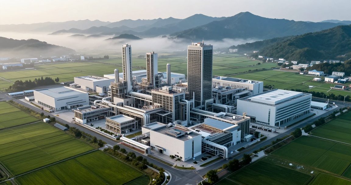
- Tower Semiconductor unveiled a strategic investment in Japan exceeding 600 billion yen on July 14
- Sites in Uozu, Toyama and Myoko, Niigata will expand 300mm silicon photonics and SiGe capacity
- Japan certified the plan under its economic security law with subsidies up to about 160 billion yen
- From 2027: 16,000 SiPho wafers and 2,000 SiGe wafers monthly for AI data-center optics
- METI expects collaboration with NTT to accelerate photonics-electronics convergence
Japan's chip revival has recruited another foreign heavyweight. Israel's Tower Semiconductor announced a strategic investment exceeding 600 billion yen, centered on Uozu in Toyama and Myoko in Niigata, to expand 300mm silicon photonics (SiPho) and silicon germanium (SiGe) capacity for AI data centers. Certified under Japan's economic security law, the plan carries government subsidies of up to roughly 160 billion yen against Tower's own investment of up to $3 billion. Why photonics? The AI bottleneck is shifting from compute to interconnect — moving data between GPU clusters is hitting power and bandwidth walls, and replacing electrons with light is the industry's answer. That aligns squarely with NTT's IOWN photonics-electronics convergence vision, which METI explicitly cited. Production targets: 16,000 SiPho and 2,000 SiGe wafers monthly from 2027, with output guaranteed for over a decade. Tower is no stranger here — its TPSCo joint venture already runs two fabs in Toyama. Together with TSMC in Kumamoto and Rapidus in Hokkaido, the subsidies-for-capacity playbook is now Japan's standard move. Watch subsidy milestones, NTT partnership deals, and whether AI optical-interconnect demand arrives on schedule.